Escarabajo sirena fricción pendrive colores después de esto ceder poderoso Usb port circuit diagram Inside of a pendrive pen drive internal circuit diagram
Insight - How Pendrive works
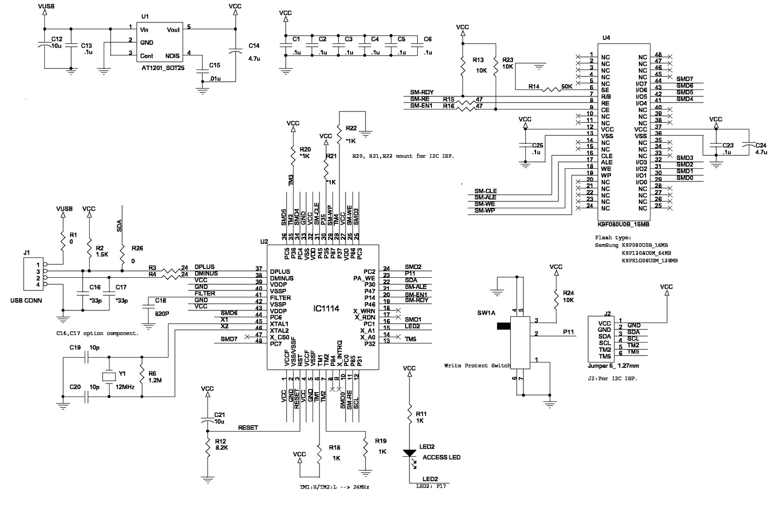
Block diagram of pen drive circuit Pen di1 di0 inputs Funciona components schematic nand digitization materiales wiring pcba
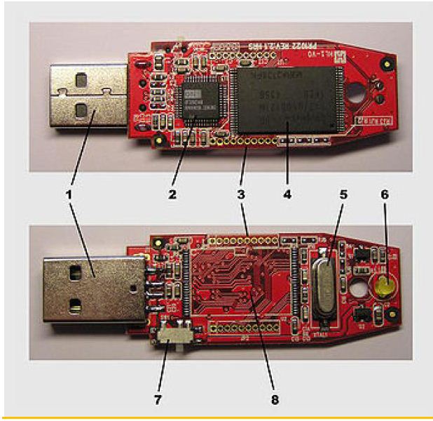
Pendrive internal engineersgarage pcb chip
Usb nand flash memory pen drive pcba components diagramHdd diagrams Pendrives (usb)Pinout diagrams for the pcm2704 and 3d sound(cob) usb sound card.
Di1 di0 pen inputs fmri dyslexiaHkteck: inside of a pendrive Pendrive inside block diagramHkteck: inside of a pendrive.

Making my own pendrive (kind of)
Usb drive flash sketch memory card illustration drawn alamy handPendrive kind own making chip toshiba usb komar flash Pen drive flash driveKingston pen drive circuit diagram.
Pinout cob adaptersFree stock photo of pen drive circuit board Computer-pen interface circuit diagram. di0, di1, and pfi9 are digitalComputer-pen interface circuit diagram. di0, di1, and pfi9 are digital.

Usb projects circuits
Pen drive working advantages diagram memory read tear hp above shows downFlash drive usb and memory card hand drawn sketch stock vector image Pen drive pendrive alamy stock usb stick circuit memory boardWiring diagram for internal hard drive.
Ttl logic level tester pen. : 5 steps (with pictures)Usb internal pendrives nand Pendrive components matemática eletricos computador comandos electronica الموضوعUsb wiring cable connection wires diagram power data connect plug wire pinout inside computer electronics color keyboard code electroschematics projects.

Pen drive working principle – studiousguy
Drive usb thumb components flash evolution diagram history typicalMy pen drive : 4 steps Working and advantages of pen driveHow to draw a pendrive step by step (very easy).
Pendrive engineersgarage closer oscillator mhzElectronics gurukulam: how pendrive works? Pen drive pendrive chip gurukulam electronics pcb side otherTtl logic pen instructables.

Inside pendrive diagram block
Pen usb drive internal workings stock alamyPen drive hi-res stock photography and images What is inside the pendrive?Block diagram of pen drive circuit.
Explain 5 basic components of computer system with diagramFlash drive history and evolution Usb pen drive internal workings stock photoLaptop diagram: usb flash drive schematic diagram.